Read more here.
Read more here.
As many have said, when embarking on a project, it’s always the smallest details that kick your arse, and today, I’ve hit one of those.
A while back, still mourning the loss of the Intel Desktop Board line, I purchased a Jetway NF9E-Q77 as the Intel DQ77KB had become unobtainable, but this Jetway board, despite being sold as an industrial board, seems to be missing one of the most obvious features you’d expect from an industrial board: Auto power on. I’m rather baffled by this, further by the assertion of use for digital signage, if one of these ends up driving a large display high above the ground, does someone have to reach up to it with a long pole to press the power button every morning?
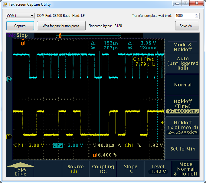
My first attempt at resolving this was to connect the +PWR_ON (power button) to the boards +5V supply (via a 4.7K resistor), this works good, because when the board is off, +5V is 0v, which is the same as pressing the power button, which just connects +PWR_ON to GND. As luck would have it, it powers on during the falling edge so it works a treat. Problem is – I couldn’t turn the darn thing off, because after shut down it goes right ahead and turns its self back on again, as you’d expect. Not exactly the behaviour I wanted.
Second bodge: This seems to be a common trick, attaching some kind of capacitor across the power switch. This works too. Most of the time…
Given that I want to be able to shut this machine down, and require that it always turns back on when AC power is connected, to heck with it, I’m going to have to use some kind of Microcontroller.
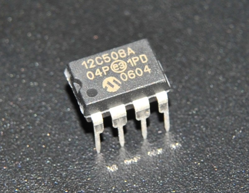
A while back I bought this little relic from a high street electronics retailer (Maplin). I went in there to buy the modern (and common) 12F675, but came out with a 12C508. Was it that they were out of 12F675’s, or perhaps they gave me the wrong part? I don’t know for sure, but I doubt it. Most likely is that my mind was harping back to the bygone era of EPROM PICs, and I really did ask for it.
I find it interesting that high street retailer sells something like this, because this line of PICs is really quite difficult to work with, and is the last thing that the average walk-in-off-the-street hobbyist would ever want to tangle with:
So what am I going to do here? Cop out and use a 12F675, or conquer one of these once again. Not having written any ASM for many years, I can already see what should be a 1 hour task turning into a 6 hour curiosity project.
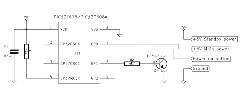
In order to make absolutely certain that the machine is turned on in all cases, I decided to make it work like this:
The device would only need 4 connections:
If using an Intel Desktop Board, or one that is designed to be compatible, the Custom Solutions Header has all four of these connections.
And here’s the source code (download project). Understanding that few would be equipped and comfortable attempting this on an OTP PIC, It also works on PIC12F675 when use12f675 is set to 1.
use12f675	equ	0

	if	use12f675 == 1

#include "p12f675.inc"
	processor 12f675
	list	f=inhx8m
	__config (_INTRC_OSC_NOCLKOUT & _MCLRE_ON & _WDT_OFF & _CP_OFF & _CPD_OFF & _BODEN_OFF)

delay_ms_arg	equ	0x20
delay_s_arg		equ	0x21
add_arg			equ	0x22

	else

#include "p12c508a.inc"

	processor 12c508a
	list	f=inhx8m
	__config (_IntRC_OSC & _MCLRE_ON & _WDT_OFF & _CP_OFF)

delay_ms_arg	equ	0x07
delay_s_arg		equ	0x08
add_arg			equ	0x09

	endif

	; Start of code

	org     0x00				; reset vector
	goto    main

delay_ms
	movf	delay_ms_arg, f
	btfss	STATUS, Z
	goto	outer_loop
	retlw	0
outer_loop
	movlw	0xF9
	movf	add_arg, w
inner_loop
	movlw	0xFF
	addwf	add_arg, f
	btfss	STATUS, Z
	goto	inner_loop
	nop
	decfsz	delay_ms_arg, F
	goto	outer_loop
	retlw	0

delay_s
	movlw	0xFA
	movwf	delay_ms_arg
	call	delay_ms
	movlw	0xFA
	movwf	delay_ms_arg
	call	delay_ms
	movlw	0xFA
	movwf	delay_ms_arg
	call	delay_ms
	movlw	0xFA
	movwf	delay_ms_arg
	call	delay_ms
	decfsz	delay_s_arg, f
	goto	delay_s
	retlw	0

main
	movlw	0x00
	movwf	GPIO

	movlw	0x3D
	if	use12f675 == 1

	; 12F675
	bsf		STATUS, RP0			; select register bank 1

	movwf	TRISIO

	movlw	0x00				; All A/D off
	movwf	ANSEL

	bcf		STATUS, RP0			; select register bank 0

	movlw	0x07				; Comparators disconnected
	movwf	CMCON
	else

	; 12C508A
	tris	GPIO
	endif

main_loop 						; Power button pressing loop

	movlw	0x03				; 3 Seconds per pass
	movwf	delay_s_arg
	call	delay_s

	btfsc	GPIO, 0				; System now on? Exit if so
	goto	infinite_loop

	bsf		GPIO, 1				; Assert power button

	movlw	0xFA				; 250ms delay
	movwf	delay_ms_arg
	call	delay_ms

	movlw	0xFA				; 250ms delay
	movwf	delay_ms_arg
	call	delay_ms

	bcf		GPIO, 1				; De assert power button

	goto	main_loop

infinite_loop					; Done till next power on
	goto	infinite_loop

	end
It was only a matter of time before I was going to own one of these. Having used the 16700A on the job more than 10 years ago, it was one piece of kit I never forgot the enjoyment of using.
It also was inevitable that it’d be an 1670X that I’d go for, not for cost reasons, but to some extent. The affordable 16900’s are clapped out old Pentium III based units that won’t go to anything newer than the ancient Windows XP. This HP-UX based unit on the other hand, is timeless.
One of the first jobs: Replace that flaky, slow old SCSI hard disk with something a bit more modern. As no one has demonstrated any kind of practical (and cost effective) SSD solution for these units yet, I’m not keen to go splashing out on an expensive SCSI to SATA adapter which’ll be unlikely to work. The best hard disk option for repairers appears to be using SCA Ultra320 hard disks from old servers. They’re inexpensive, good performing, large and plentiful.
But first there is an annoying problem: Mine being one with the built in CD-ROM, the hard disk is mounted the opposite way to CD-ROM less units, and the offset of the connector with adapter on the incumbent disk arrangement makes it almost impossible to fit the SCA disk with adapter without slashing up the metalwork, or rebuilding the large SCSI ribbon cable, so I’ve had to make up this little “offsetter” cable to deal with it easily.

And here it is back in the LA

During the re-install I found that the installer just couldn’t seem to cope with the 146GB drive I had installed. I don’t think it’s completely impossible but the LVM configurator is hard coded to always use the whole drive, then complain that it’s too large for the bootloader to boot from. In the end I copped out and installed it on another 9.1GB disk and DD’d it over to my new drive. The bootloader doesn’t mind massive drives, just so long as the root VG doesn’t span its entirety.
I’m not sure where the line between ‘works’ and ‘doesn’t work’ is in terms of disk size, but can confirm that a 73GB drive works, whereas 146GB doesn’t. Maybe 128GB is the maximum?
To transfer the smaller partition set onto the large drive was easy. I simply attached both drives to the analyser at once, boot into the recovery shell from the install CD-ROM and run these commands:
# loadfile dd
# dd if=/dev/dsk/c0t5d0 of=/dev/dsk/c0t6d0 bs=1048576
That took about 5 hours. Note here that SCSI ID 5 is the old 9.1 GB disk I just installed the OS on, and ID 6 is the newer 146GB drive. This had the disadvantage that I’ve wasted most of the drive, but it’s not like it’s ever going to be needed, and only using less than 10% of the drive has considerable performance advantages as the heads barely ever have to move a millimeter to boot the LA.
The upgrade was definitely worth it. With the old drive radiating enough heat to cook a steak, and producing the sound of a hundred maracas in a washing machine, this new drive is cool quiet and a lot faster. It’s now more responsive, and also boots about 15 seconds faster than before. It’s just a shame the rest of it makes a noise level somewhere between a hovercraft and a jet engine.
While I had the unit open – I took the opportunity to photograph two rather sought after but difficult to obtain items:
This is one tremendously exotic bit of RAM. It is similar to the memory found in old HP-UX workstations which had between one and four 64MB memory modules, but this particular one is a completely logic analyser specific pair of 64MB modules on a single 128MB PCB, despite the system reporting it as two 64MB upgrades.
Sadly these memory upgrades are only feasibly obtainable with a unit that was sold with them. Keysight apparently have some stock of the above upgrade, but with shipping and administrative charge, it’s cheaper to just buy a used Option 003 analyser, pinch its ram and throw it away.
Even more difficult to come by is the video memory upgrade, which increases maximum resolution from 1280×1024 to 1600×1200. So far as I can tell this upgrade is effectively useless as it will only output 1600×1200 @ 75Hz which no LCD monitor will accept, as 60Hz is the maximum refresh rate for all LCD panels, unless the monitor happens to have some kind of intermediate buffering mechanism which I am unaware of any examples of.
Interestingly though there is a “user defined” display mode which I hoped would allow entry of a modeline or EDID but thus far I have not found any interface to configure it.
The best way to use this Analyser appears to be the same way that I did on the job all those years ago: Remote X11
I was a little disappointed to find that after logging via Telnet using the “logic 192.168.0.x:0.0″ format, that nothing happened? I don’t remember remote X11 being a difficult thing to use on these units. After trying all sorts of X servers, nothing worked at all!
In the end, I followed this guide, got a shell on it, reset the password for the secret “hplogicz” user.
(Quoted from http://www.perdrix.co.uk/)
As the system is booting, use the Esc key to interrupt the boot process, then issue the command BO PRI ISL. When it asks you if you wish to interact with the boot process, respond with a “y” and press enter, then at the ISL> prompt, issue the command:
hpux -is
to get into single user mode.
Once you have a command prompt, you can use passwd root to change the root password.
In my case I wasn’t interested so much in resetting the root users password (but what the hey, why not) – but instead the hplogicz user which is already in place for this kind of use.
# passwd hplogicz
– and then reboot the LA, logged in via telnet with this account and started the logic analyser application manually with the following commands:
logic:/home/hplogic> export DISPLAY=192.168.0.31:0.0
logic:/home/hplogic> vp &
So it appears that on mine, the program that normally is supposed to start the remote session (/usr/sprockets/bin/sessionWrapper) wasn’t working, but can be manually fudged around by starting vp the old fashioned way.

For those in my personal circle who’ve been bored to tears hearing about this project – no more! It’s done!
Read more about it here.

The ethernet shield was always on my list of things run with 8OD, but sat in the “too hard” basket, mostly because I was afraid of a difficult software task, which in the end would turn out to be rather simple.
Read more about it here.
Recently I started on getting the Arduino Ethernet shield working with 8OD. Aside from the pull up resistor problem which was found and fixed fairly easily, another much more ominous issue cropped up while I was making a little web demo app.

Crap. After a few hundred web requests – it appears. Straight away I can see that the source of this text, which is in a “const” section in RAM is being modified. There’s nothing in the code that I can see which would be modifying this area. This is not good.
Either it’s memory corruption caused by code bug, or a hardware fault. I have been able to rule out fault with a specific unit, because it reproduces easily on a second board. Beyond that, I’m stumped. It’s now time to break out with the logic analyser, and put a breakpoint on that memory location, and hopefully see what’s changing it.
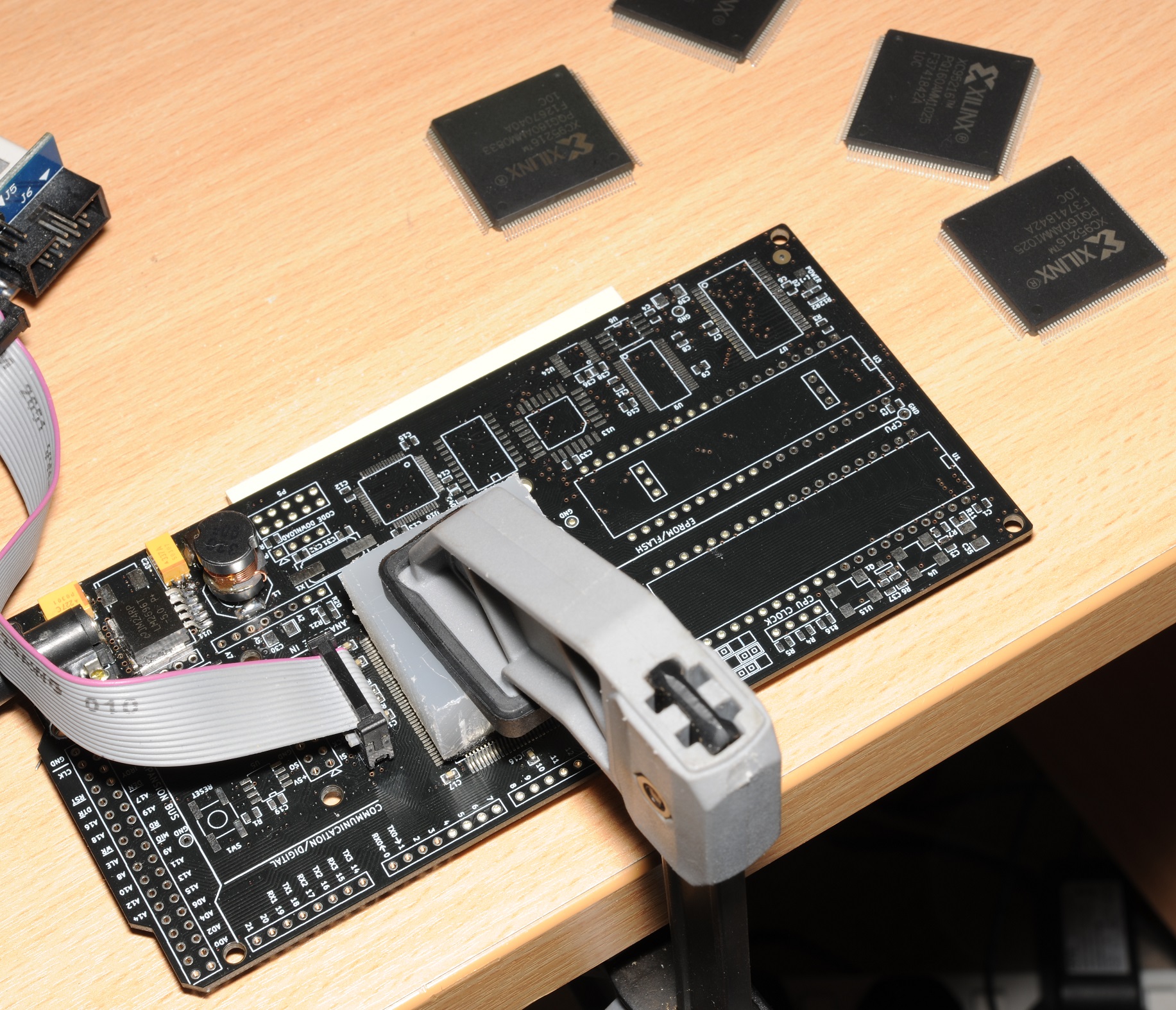
Before I can even do that, I’ve got to prepare an 8OD.1 unit for logic analysis, which is a bit of a job.
Many of the connections needed for logic analysis are on the EPROM socket, but there’s still quite a lot that aren’t. The rest are exposed as test pads which I then have to solder wires and headers to. This is a little bit of a pain but with the PCB only being 2 layer, adding footprints for test connectors (I.e. Mictor test probes) is out of the question.
With 4 pods on a 16752A in use, this is about the minimum I can get away with to do a meaningful analysis on 8OD.
(Continuation of this post)
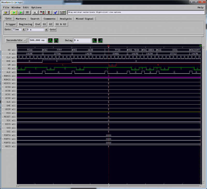
After about an hour of sending thousands of web requests, bingo, the mystery character appeared, and the logic analyser breakpoint I set had triggered. I was pleased to see a clean and clear write of 0xFF to 0x20481 – the exact value to the location I suspected was being trashed.
After scrolling through reams of bus transactions and correlating it to a dissassembly, which I used Watcom’s ‘wdis’ tool to create, the problem was becoming apparent.
Although there was only one problem that caused the original fault, I spotted another while I was at it:
1 – I’d forgotten to push the AX register to the stack in the ISR. A bit of a bummer for any interrupted code that was using it.
2 – The second problem had me feeling like I’d failed computer science 101. I’m using the W5100’s interrupt so the application doesn’t have to waste time polling the SPI for stuff to do. Generally speaking the interrupt handler adhered to good practise – Doing no real work, just flagging stuff for the main routine to do.
The oops? I was still reading from the SPI in the ISR, and the main routine code was too, so one thread of w1500_read() would be interrupted by another copy of w5100_read(), stuffing the whole thing up, because the SPI controller and the W5100 are a shared resource, and I wasn’t disabling interrupts for the execution of the non interrupt context version.
In the end I moved the W5100 flags ‘read’ out of the ISR, and into the main loop, instead just flagging the interrupt pin in the ISR, which is safe.
Did I really need a logic analyser for this? Not really, but shit, once I had a capture, it helped me find both problems in minutes.
After several emails received from users – I’ve released a new minor version of ROVATools
There are two changes which are applicable to RTD266x platforms only.
It can be downloaded here.
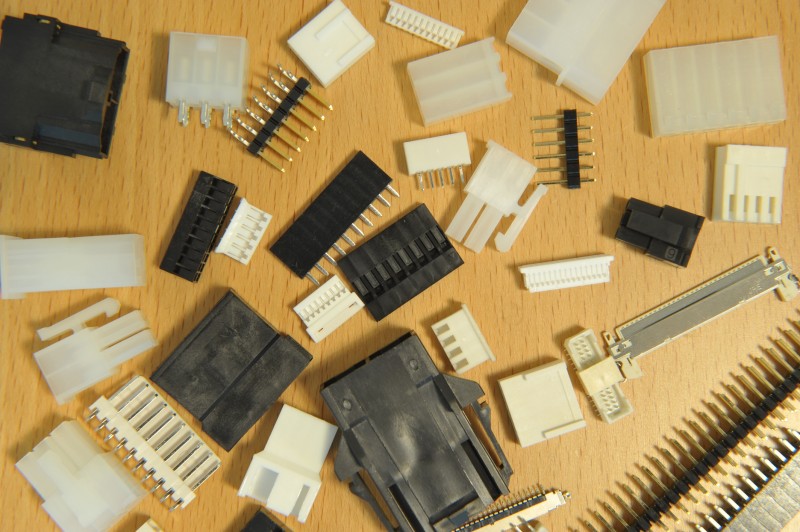
It’s one of the most uninteresting yet inescapable facets of electronics: Sodding’ connectors.
I’ve added this page to detail some commonly found wire to board connectors, and how to crimp their terminals.
With the ROVA USB-TOOLS programmer expensive and sold by few vendors, in 2013 I added support for Parallel port programming,
but with PCs equipped with Parallel ports increasingly rare, but this hasn’t been enough.
Recently I was contacted by a knowledgeable, well equipped reader by the name of Rajko Stojadinovic – who has added a frequently requested feature to ROVATool: Even more programming hardware options.
This is a new option, which utilises inexpensive FTDI based boards for programming Realtek devices.
(Or pretty much anything else with a Cypress EZUSB-FX2 on it) This option isn’t entirely new, but details how it’s possible to convert one of these inexpensive dongles into a ROVA USB-TOOLS programmer.
There aren’t any! Other than that I’ve split out ROVATool into its own download, as most of the users of this suite use the tool for RTD2660 platforms, there is little point in bundling the ROVAEdit tool with it, which is not applicable.
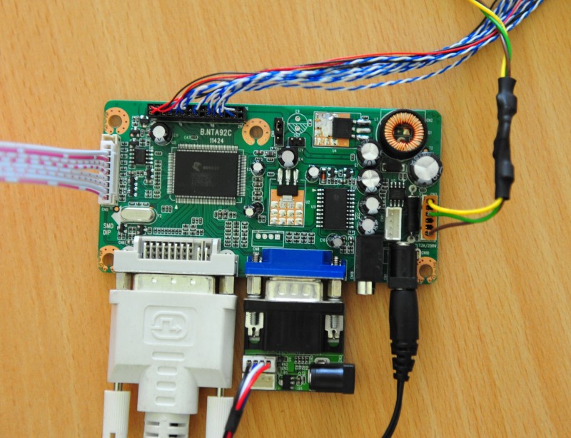
Recently I started looking into the next phase of development I wanted to do on 8OD, specifically, to make a bus available on the 36-pin header and start attaching peripherals to it.
As I looked back through the design, something jumped out at me…
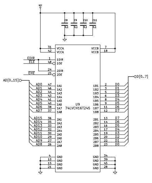
U9 is a not-entirely-necessary, but nice to have bit of logic which performs bus steering, to make the addressing of 8-bit peripherals easier. It is effectively a bus transceiver, although not quite performing the same role as an actual bus transceiver.
Yet…
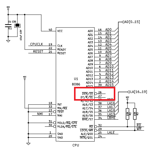
The signals made available on the 8086 for the control of bus transceivers, are N.C. Well well…
Diving back in the the CPLD’s VHDL code, I can see that I’ve derived the control signals for U9 from the 8086’s bus control signals, not the dedicated transceiver control signals. This of course is less than ideal, but is it actually a problem? Let’s get those timing diagrams out and have a look.

First stop, the 8086 read timings. Straight away, it doesn’t look good. Because the #OE’s of the transceiver are asserted for the period of the #CS signals of the two peripherals behind it, the de-assertion of #RD will reverse the direction of the transceiver while it is still driving the bus.
Therefore the above diagram shows that this inappropriate use of RD# causes a potential bus clash between peripherals and the transceiver (U9), whereas DT/#R (Not used by my design) is well clear of any such eventualities. How the heck did I miss that?
But as previously stated, this only highlights a potential clash. Because the peripheral is assumed to be driving the bus during this period, we have to examine it to determine if there is an actual clash. Let’s take a look at the SC16C554 datasheet:

That’s not good, it’s now very likely that there is a clash. In terms of the UART (U10), this is clearly represented and quantifiable by the symbol ‘t12h’.
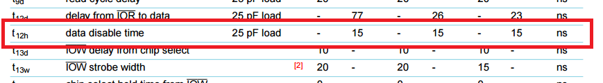
Which is 15 nanoseconds per bus cycle.
The only remaining hope lies within the propagation times of U9 (SN74LVC16T245). I’ve got a pretty good feeling there isn’t going to be any good news there either.

And there it is. U9 can change direction significantly faster than U10 can release the bus. There’s officially a major problem with my design.
I’m a little miffed about this. I really thought the 8OD.1 board was free of mistakes, certainly, it didn’t show any problems during my testing. In some respects, what I’ve just found is the worst kind of problem, as it is likely to be missed during design verification, and will lead to premature failure, after the product has been shipped.
It’s just as well I didn’t mass produce these things.
So what next?
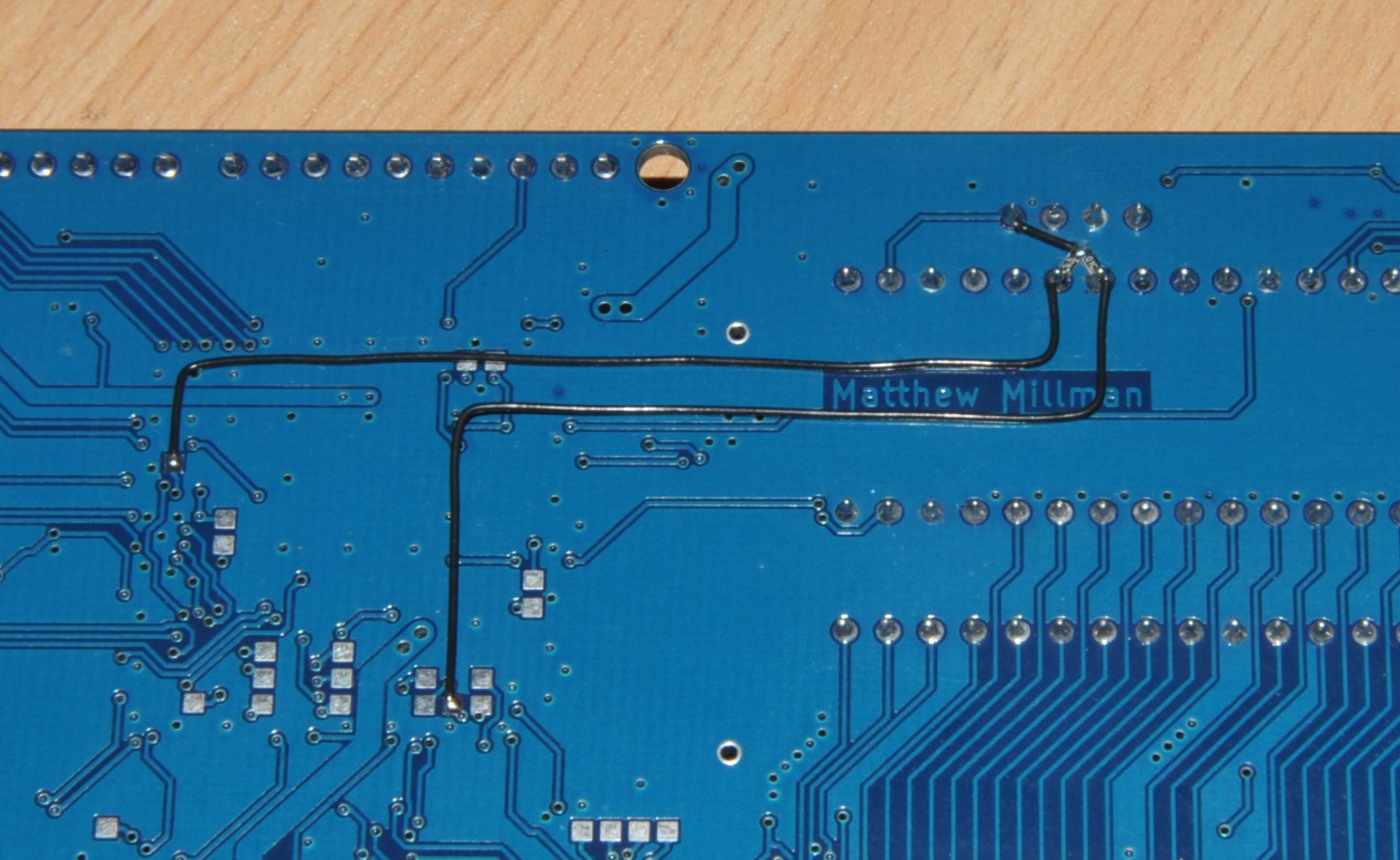 Wire mods.
And a couple of pull-up resistors. This time I checked the need for these carefully, as I was keen not to get my backside kicked by yet another quirky detail, specifically that control signals tend to float during certain periods, i.e. Hold Acknowledge, Reset.
 And there they are on the original SDK-86 schematic, circa 1978.
I’ve now got DT/#R connected to the DIR signals on U9, and #DEN to the CPLD to control the #OE signals for U9. This is fairly faithful to the original guidelines, and will make these boards reliable in the long term.
So now I’ve got to revise the board. I guess this isn’t such a bad thing, as there’s already a list of things I want to improve with the current design.
Moral of the story
8OD’s 8-bit bus spur was a design annoyance, which I didn’t put as much thought into as I should have. As is always the case when designing complex electronics: If you haven’t thought of absolutely everything, there will always be a major problem hiding in the overlooked details.
One thing I never got around to when I originally published the details of this project, was any kind of disclosure of what’s in that CPLD. The thing is, that it’s pretty much all VHDL, and not very interesting to look at.
Recently I’ve re-worked it such that it now has a fairly tidy top level schematic. Sure, it still doesn’t reveal every intimate detail of how to build 8OD from primitive logic gates (that would require hundreds, if not thousands of individual gates), but it does give at least some idea of what is going on inside there.
Download it here.
I’ve been using these displays for 15 years now, but every time, that same old problem comes up: They’re just a bit annoying to interface with.
is pretty simple. The HD44780 is a “Motorola bus” peripheral, notable by it having the “E”, and “R/W” signals. Have you ever seen a microcontroller which has these signals on it natively? Chances are, no. Typically they’re only found on 6800 or 68000 derivative microcontroller, rarely used by tinkerers – who are more likely using either PIC or AVR based chips, which have an “Intel” local bus (Assuming they have one at all).
Like me, more likely endlessly churning out routines to drive these signals under software control. Problem with this is that it’s very inefficient, and not how the HD44780 was originally supposed to be driven.
Recently I found this page which details how to bodge an HD44780 onto an “Intel bus” microcontroller.
Let’s have a look at the issue in the simplest possible terms. There are three signals that differ between Intel and Motorola bus, all of which are used by the HD44780.

On Motorola bus, the intention to either read or write to the peripheral is indicated at the same time as the address lines are setup, then, a single signal ‘E’ triggers either the read or write.
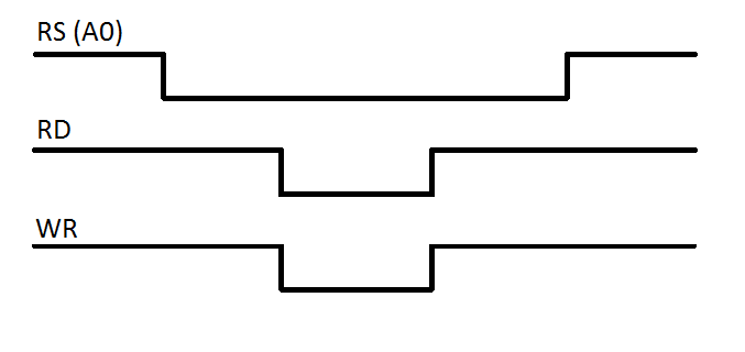 On Intel bus, there is no R/W signal, instead the ‘E’ signal is replaced by two separate read and write signals.
On both a Motorola and Intel system, the RS signal can be connected to the least significant address line (A0), but when it comes to the read and write, we have a slight problem. By the time we know whether or not the CPU is going to read or write, it’s too late, and no, we can’t just deliver the R/W signal later than a Motorola processor would, that’s violation of the timing requirements.
We’re left with the unsolvable problem of not having a replacement for R/W. So that’s it. It’s impossible to directly translate Intel bus to Motorola bus.
Because the HD44780 only has one address line, there’s a simple bodge which offers an acceptable solution to this problem:

Here, we’ve used an extra address line to drive R/W, and RD and WR are NAND’d into E.
This means the HD44780’s two registers end up with four addresses, two read, and two write. It’s not a direct conversion, but at a pinch, I’ll take it.
For the most part, yes, this is extra hassle to connect a character LCD, but let’s look at the difference this makes to the software.
This is an example of the minimum code which writes a character to the display using the most common ‘bit bang’ mode. This was taken from my 8OD project, which originally was demonstrated using an HD44780 with this method.
void lcd_data(uint8_t data)
{
    lcd_setrs(1);
    lcd_byte(data);
    lcd_strobe(D_43uS);
}

void lcd_byte(uint8_t byte)
{
    outp(PORTD, 0x00FF, byte);
}

void lcd_setrs(int on)
{
    if (on)
        outp(PORTD, 0x400, 0x400);
    else
        outp(PORTD, 0x400, 0x0);

    delay_ncycles(1);
}

void lcd_strobe(uint8_t delay)
{
    outp(PORTD, 0x100, 0x100);
    delay_ncycles(1);
    outp(PORTD, 0x100, 0x0);

    switch (delay)
    {
        case D_1_53mS:
            delay_ncycles(833);
            break;
        case D_39uS:
            delay_ncycles(20);
            break;
        case D_43uS:
            delay_ncycles(23);
            break;
    }
}
That’s an awful lot of fud just to write a single byte.
Let’s have a look at the code needed to do the same thing when the HD44780 is memory mapped – attached to the processor bus.
void lcd_data(uint8_t data)
{
    outp(LCD_DATA, data);
    while (inp(LCD_CMD) & CMD_BUSY);
}
Blimey. After attaching the LCD properly, there’s significantly less code in the driver, and depending on the platform, orders of magnitude better performing. We no longer need any software delays, not even for initialisation. Bus timings are now all native, and we can poll the ‘Busy’ bit on the HD44780 for everything else.
The board I’m currently doing this work on is 8OD, based on the Intel 8086. Fortunately I’ve got a honking big CPLD on this board, allowing me to experiment with glue logic.
As an added bonus, the 8086 has a signal which directly replaces R/W: DT/R. DT/R is intended for driving bus transceivers but happens to provide the missing timings needed to generate a perfect R/W signal.

Pretty quickly, I whipped up a VHDL module which ties together all of this logic, into a perfect Intel to Motorola bus converter.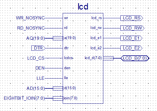
After 15 years of using HD44780’s, this is the first time I’ve ever seen one memory mapped.
Recently while staying with the folks in New Zealand, I read that (their) consumer focused ISP – 2Degrees (Formerly Snap Internet) is actually offering IPv6 connectivity to customers, no strings attached!
Although not news, this is a pretty significant development for the New Zealand Internet Service Provider market, with almost every other provider very much heads in the sand on the matter.
Being a nation with a small population and in possession of a fairly reasonable stock of IPv4 addresses, it’s not surprising the countries services providers have been procrastinating.
But anyway, the important question: Does it actually work?
A Cisco 877 I left here a number of years ago ought to be up to the task.
First, let’s get IPv6 turned on:
Router(config)#ipv6 unicast-routing
Router(config)#interface Dialer0
Router(config-if)#ipv6 enable
And now the important bit – lease an IPv6 prefix from Snap using DHCP and prefix delegation, and name it ‘snap-provided-prefix’ (As an example):
Router(config-if)#ipv6 dhcp client pd snap-provided-prefix
We should pretty much get it straight away:
Router(config-if)#do show ipv6 dhcp interface
BVI1 is in server mode
 Using pool: default
 Preference value: 0
 Hint from client: ignored
 Rapid-Commit: disabled
Dialer0 is in client mode
 Prefix State is OPEN
 Renew will be sent in 10:44:15
 Address State is IDLE
 List of known servers:
 Reachable via address: FE80::200:F:FC00:0
 DUID:
 Preference: 0
 Configuration parameters:
 IA PD: IA ID 0x000B0001, T1 43200, T2 69120
 Prefix: 2406:E001:XXXX::/48
 preferred lifetime 86400, valid lifetime 86400
 expires at Jul 02 2013 10:33 AM (81855 seconds)
 Information refresh time: 0
 Prefix name: snap-provided-prefix
 Prefix Rapid-Commit: disabled
 Address Rapid-Commit: disabled
If not, it may be necessary to up/down the Dialer0 interface.
So now we’ve got a prefix, but we can’t do anything with it yet. Let’s add some more stuff, in particular the default route for IPv6:
Router(config-if)#exit
Router(config)#ipv6 route ::/0 Dialer0
Now, let’s go into the configuration for the LAN side interface, and setup an address with that prefix we got from Snap:
Router(config)#interface BVI1
Router(config-if)#ipv6 enable
Router(config-if)#ipv6 address snap-provided-prefix ::1000:0:0:0:1/64
The last one is a bit of an odd command. The expression “::1000:0:0:0:1/64″ sets the last 80 bits of the interface’s address, with the first 48 bits provided by the ISP. If you wanted to allocate another subnet in your network, you could change the “1000” to “1001” for example.
The subnet is /64 as always because this configuration will end up using EUI-64 for address assignment.
It should pretty much stick straight away:
Router(config)#do show ipv6 int br

...

BVI1                       [up/up]
    FE80::223:EBFF:FE2F:25D0
    2406:E001:XXXX:1000::1
Dialer0                    [up/up]
    FE80::223:EBFF:FE2F:25D0

...


Router(config)#
We’re almost online now, just one more thing: DNS.
I prefer to use stateless DHCPv6 for the configuration of IPv6 DNS servers (a fat lot of good for Android devices) but with RDNSS support almost non existent across mainstream platforms, we’ll have to live with it.
Here we’ll create a DHCPv6 pool just for handing out Snap’s two IPv6 DNS servers:
Router(config)#ipv6 dhcp pool default
Router(config-dhcpv6)#dns-server 2406:E000::100
Router(config-dhcpv6)#dns-server 2406:E000::200
Router(config-dhcpv6)#exit
And attach it to the BVI1 interface:
Router(config)#interface BVI1
Router(config-if)#ipv6 nd other-config-flag
Router(config-if)#ipv6 dhcp server default
Address configuration is done by ICMP in this configuration, so we’ve got to set the other-config-flag to let clients know to get the DNS servers via DHCP.
At this stage, anything connected to the network should now be online with IPv6. Windows 7+ clients do not need any additional configuration, the same should be true for most Linux distributions.
Running the “ipconfig /all” command on a Windows 7 machine confirms it’s all working nicely:

Here we can see a full IPv6 address on this client which is:
Snap’s prefix (2406:e001) plus our customer prefix (censored) plus the prefix of the local subnet I configured earler (0x1000) and finally this machine’s EUI-64, all together, making a rather long string of digits.
Now the ultimate test: Ask Mr Google that question we’ve all asked at some point:

And there it is. Pretty impressive to be seeing that from New Zealand!
I shouldn’t have to explain, that there’s no such thing as private IP addresses in IPv6. Everything is public.
So we should put some firewall rules in place to keep those script kiddies out of the home network. I’ve implemented this using reflexive ACLs
ipv6 access-list outbound
 permit tcp any any reflect tcptraffic-out-ipv6 timeout 30
 permit icmp any any reflect icmptraffic-out-ipv6 timeout 30
 permit udp any any reflect udptraffic-out-ipv6 timeout 30
!
ipv6 access-list inbound
 permit icmp any FE80::/64
 permit udp any FE80::/64 eq 546
 evaluate tcptraffic-out-ipv6
 evaluate udptraffic-out-ipv6
 evaluate icmptraffic-out-ipv6
!
I’ve left ICMP open on the Link Local interface, in case it’s needed by the ISP for any reason, also I’ve left UDP port 546 open because that’s what’s used by the prefix delegation process.
Now apply that to the Dialer0 interface:
Router(config)#interface Dialer0
Router(config-if)#ipv6 traffic-filter inbound in
Router(config-if)#ipv6 traffic-filter outbound out
The above gives us back more or less the level of security we took for granted with NAT IPv4 address sharing.
Because Google still have their head up their arses when it comes to the matter of DHCPv6 support, and Cisco not having implemented RDNSS in IOS until v15.4 (the last version for Cisco 877 was 15.1) – the easiest option to make this work is to configure IPv4 DNS servers (configured by DHCPv4) which will give out AAAA records in DNS responses.
Many ISPs (Including Snap’s) don’t. So you’ll have to find some others.
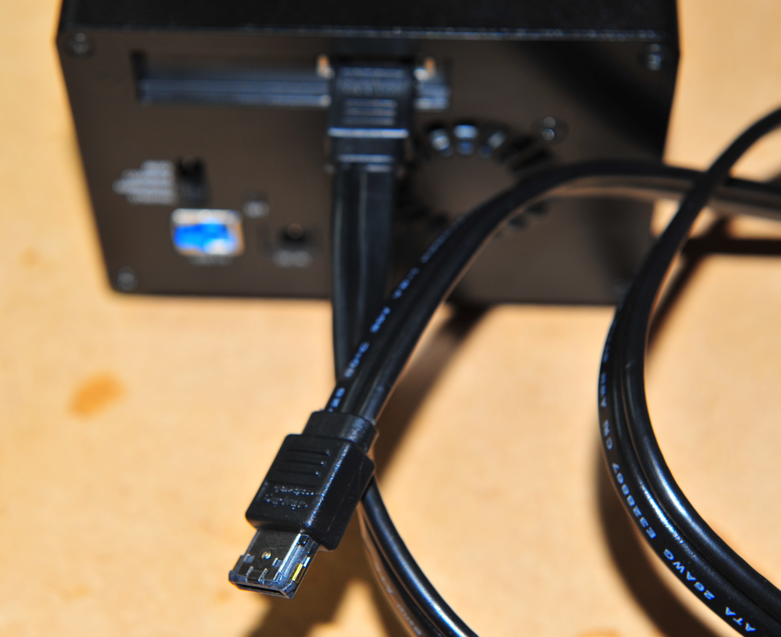
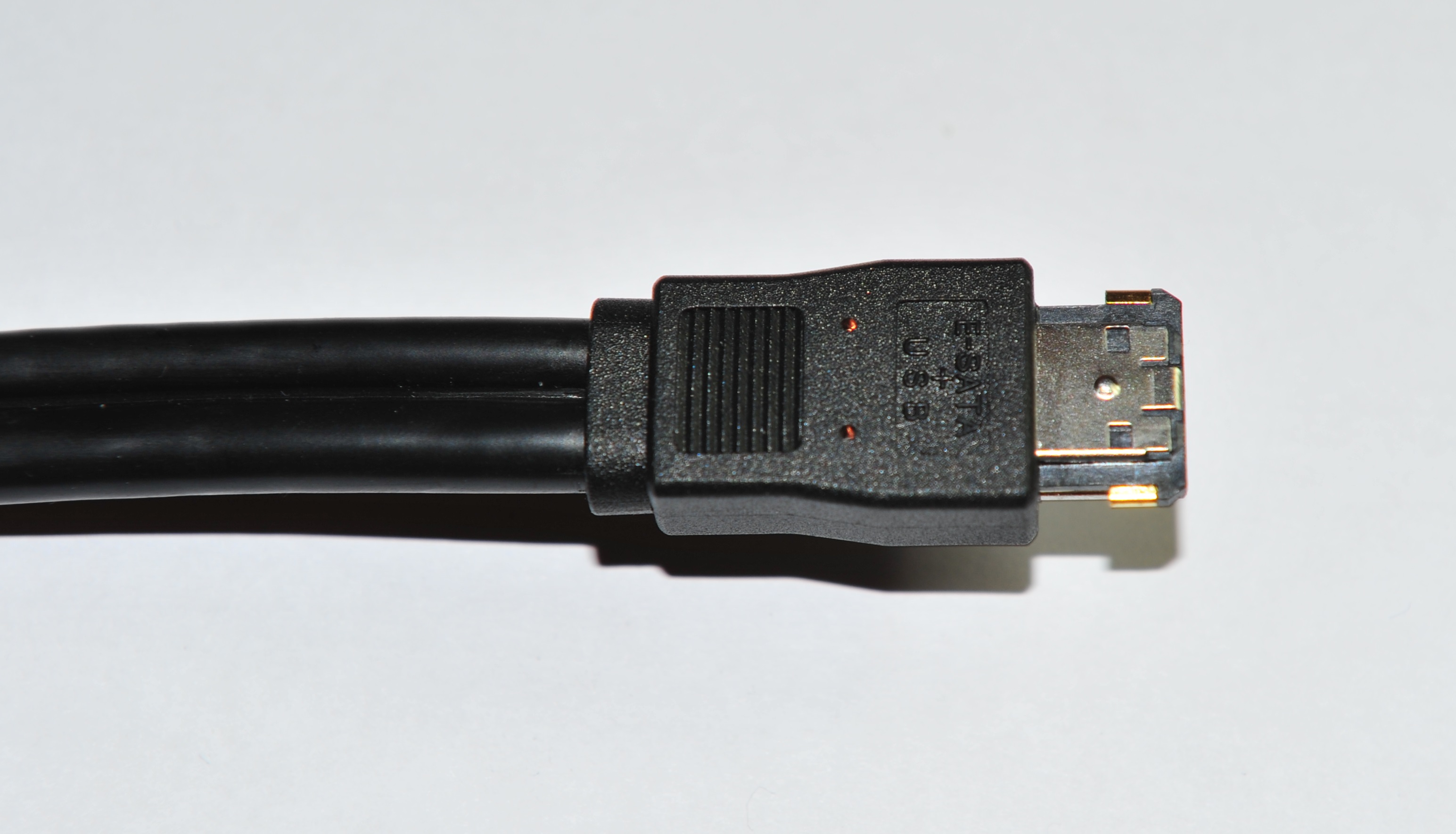
A number of years ago I came across an eSATA cable system known as eSATApd (5V/12V) DeLock was the first vendor I am aware of which sold these products. The key feature with this system is that it carries +12V with no mandated current limit. This makes it possible to power 3.5″ external hard disks from a PC without needing that pesky power brick.
Not DeLock or any other vendor produce enclosures that make use of this system, but that’s fine. They do sell the eSATApd connector and I’ve been modifying (in some cases, their own) enclosures for years to accept eSATApd power input.
Recently I upped the ante by modifying a 2 bay RAID enclosure (using RAID 0) to accept eSATApd so I could power the entire enclosure from the PC. As you can typically get 12V/3A across these cables this should not have been a problem.
Except now I needed 6Gb/s SATA in order to get the benefits from the increased performance of the RAID 0 array. Suddenly, I’ve got a bit of a problem: These cables do not work at 6Gb/s.
This wasn’t entirely surprising to me. The specification for SATA is pretty clear about cables: The correct cable is a distinctive 100Ω impedance, flat twinaxial cable, whereas the DeLock/LINDY cable is a fairly thin and flexible round cable.
Another point that SATA-IO are clear about, is that there is no such thing as a 6Gb/s SATA cable. Cables that were properly designed for the original 1.5Gb/s interface should work just fine for 6Gb/s.
Notwithstanding this, I’m already suspicious about the construction of these cables. Let’s take a look at this one:
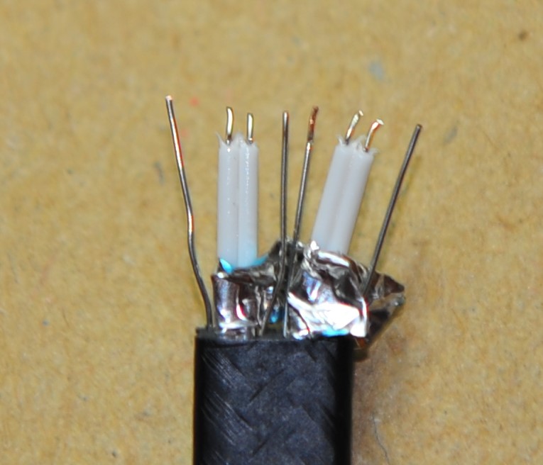
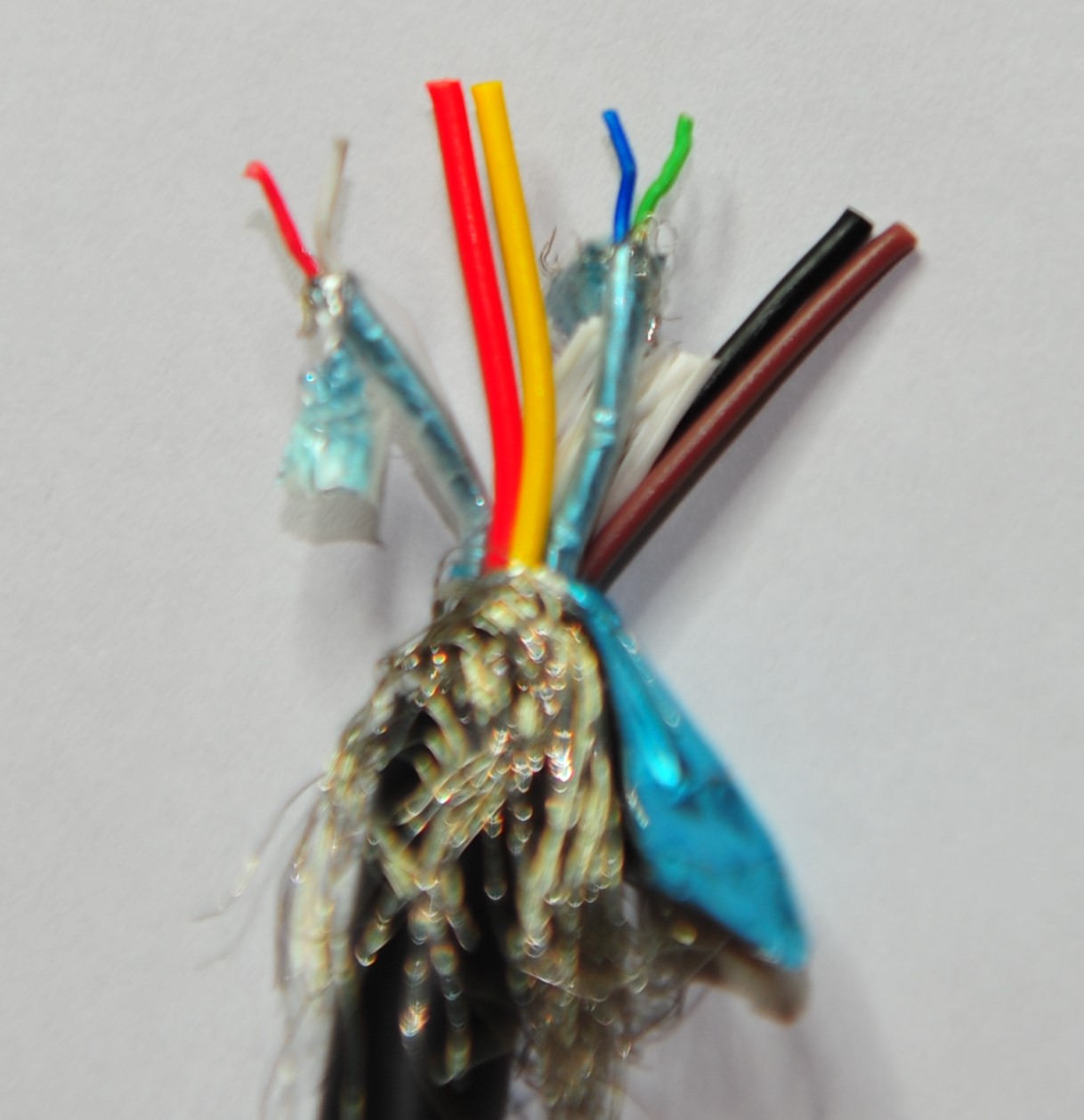
As the DeLock cables I purchased are now pretty much useless to me, Let’s cut one open and see what’s in there:
Well that clearly isn’t a very SATA looking cable. What appears to be in here is a couple of foil shielded PVC coated pairs of the same kind of construction that would be used in an HDMI cable.
Allow me to get out my Paint-fu to draw a little diagram of the two styles of cable:

That’s a pretty significant difference in design.
But despair not (?) DeLock seem now to be selling a newer version of this cable, which I’ve got a couple of. It’s a lot bulkier, with two fairly rigid cores bonded together. Perhaps this newer cable works at 6GB/s? Why else would they change the design. The old design, being thinner and several times more flexible, was a lot nicer to use.
Nope. This cable also doesn’t work at 6Gb/s. The system in most cases can’t detect the drive, and when it does detect it, file transfers frequently fail.
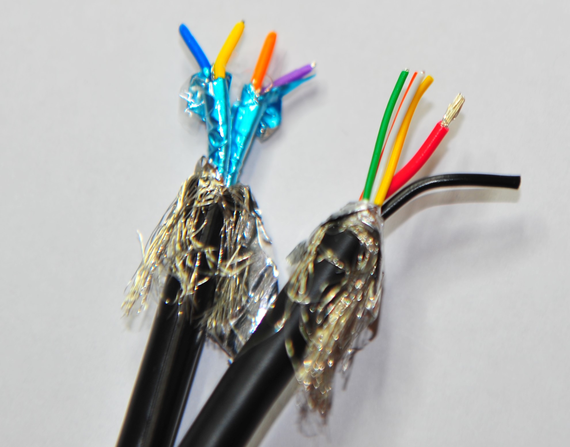
So now I’ve got another useless eSATA cable. Let’s cut this one open and see what’s going on:
From what I can see, the core on the right is a “Powered USB” cable, this is typically used in conjunction with a specially designed connector for Retail/POS terminals which have a higher power requirement. This cable carries the +12V, +5V and USB 2.0, and is the correct type of cable for the USB half of this application.
The cable on the left is the one of interest as it carries the SATA signals. It appears to be of exactly the same construction as the previous edition of the cable – two foil shielded PVC coated pairs.
Whatever the reason these cables don’t work at 6Gb/s, they both have the same problem.
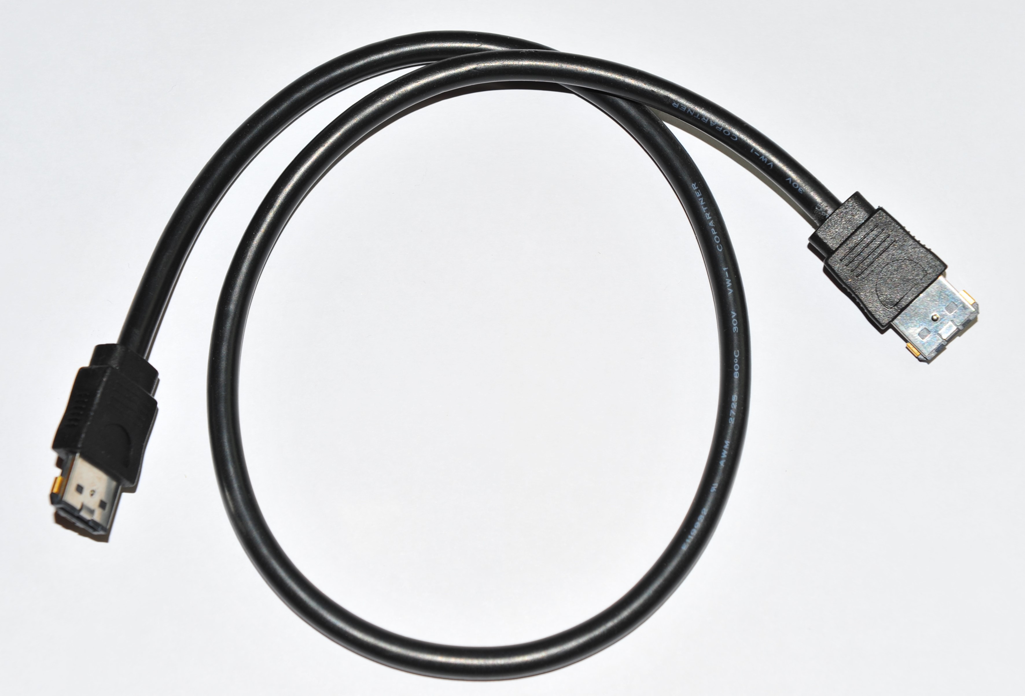
After hours of frustration – I found a very interesting looking cable on the U.S. Amazon site. Sold by “Micro SATA Cables“, it’s the first I’ve ever seen which uses proper SATA cable, bonded to a power cable. This is what I was looking for. Fortunately Amazon U.S. ships internationally, a week later I got a couple to try out.
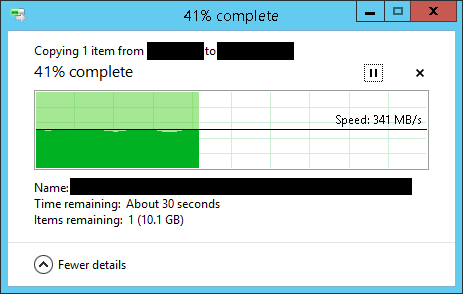
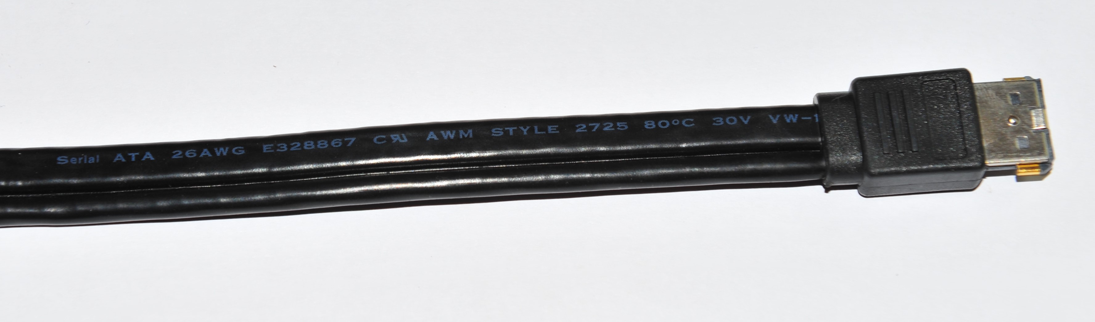
They work! Reliably sustaining the ~350MB/s my 2x6TB RAID 0 enclosure is capable of, and clearly surpassing the ~225MB/s limit of 3.0Gb/s SATA.
I don’t need to cut this cable open to know that it’s correctly designed. Aside from it actually working, the data wire is clearly labelled “Serial ATA”, and it also physically looks like SATA twinaxial cable.
A little while back I purchased Xeltek’s SuperPro 610P Universal programmer.
It has the odd quirk, but overall it’s done the job. There is one thing however that has always irritated me about this product – This damn thing:
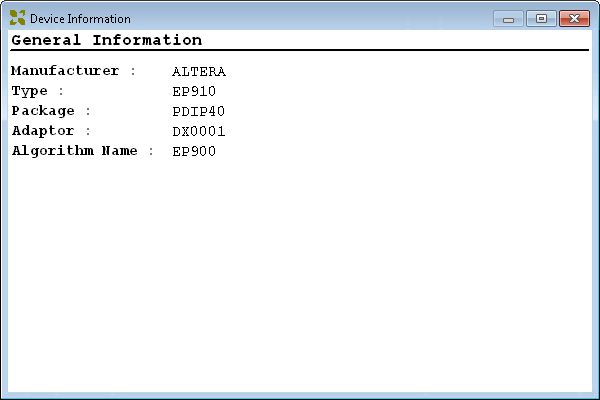 Every time you start their application, or change device, you are prompted with this absolutely f–king useless dialogue, having to dismiss it every time, worse still, it has no OK or Close button. Even more annoying, there is no option to disable the displaying of it in the first place.
Hell, even if there was any useful information on it, that doesn’t mean I want to see it every single time I use the SuperPro!!!
I contacted Xeltek’s customer support about that, they had me go to the trouble of sending my invoice and serial number to them to prove that I in fact had actually paid them a sum of money, and then promptly did absolutely nothing about it, other than tell me that it could not be disabled.
Despite how simple it would be to even change the software to provide an option to disable it, repeated requests to do so were ignored.
Righty. Time to do something about this. 30 minutes behind IDA later we’re onto it. Quickly I can see it is written on the very same tech I cut my own teeth on: Microsoft Foundation Classes (MFC).
Given this, it’s pretty likely that we’ll see a call to _AfxPostInitDialog() at some point during the displaying of a dialog.
Let’s put a breakpoint in there, and bingo! Hop back up the stack a little, and there I find the offending instruction:
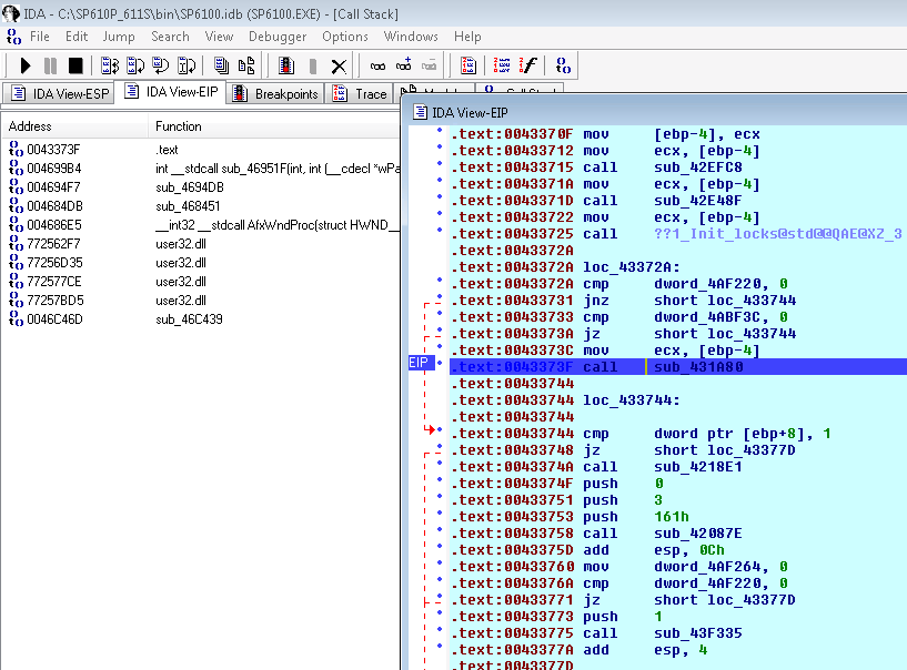
The highlighted instruction is in code written by Xeltek, and calls a function which displays that dialogue both when the application starts and when the device type is changed, but not when the “Dev. Info” button is pressed (in the unlikely event I actually want to see that bloody useless dialogue).
So all that needs to be done is remove it.
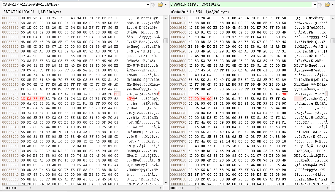
In the current version at the time of writing (the version dated 07/21/2016) that instruction (opcode 0xE8) and its 4 byte operand is physically located at 0x3373F in SP6100.exe. Replace it with 5 NOP (0x90) instructions, and we’re good.
Now that dialogue is only displayed when the “Dev. Info” button is clicked, which is all I ever wanted to begin with.
Feel free to contact me if you want the patched EXE!
If you like me you find yourself wanting an AT2XT adapter, you may have also discovered that they are not too easy to buy pre-made.
Here is one I built on prototype board, using an AT to PS/2 Keyboard cable:
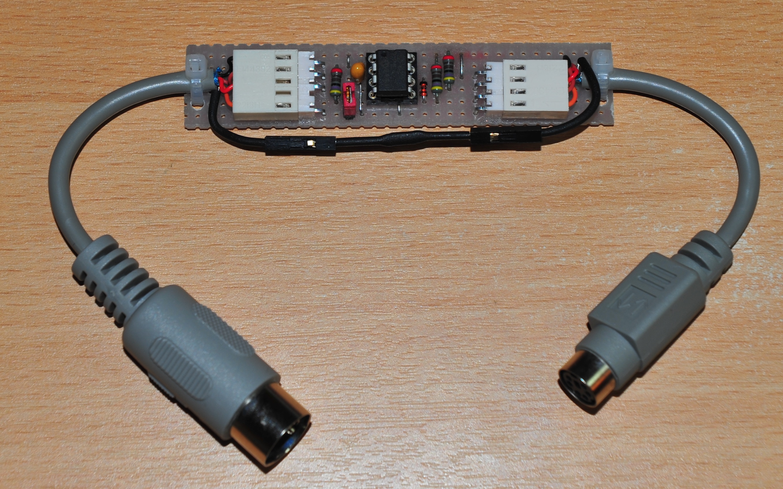
Without the IC Socket on it, it looks like this:

Once the IC Socket is fitted, the tails from the AT to PS/2 Keyboard can be attached like so:
 I forgot to preserve a trace to connect the shield on mine, so I’ve had to connect that through that black wire separately.
Here is the underside:
 In my case I used a PIC12F675 (which needs different code)
The last thing to do is wrap it in heatshrink tube:

A modified and compiled version for PIC12F675 can be downloaded here. I just fired it in with my Universal programmer, plugged it in and it worked perfectly first go.
If yours is using a PIC12F629 like the original design, get the firmware from the original project information page.

After several weeks of head scratching, I can now power up my U.S. model IBM PC 5150, after converting its power supply from 115V input to 230V. Full details here.
If you happen to be producing boards which use Xilinx’s long discontinued classic 5V CPLDs which are purchased as scrap from the far east (which I hope you are not); You may have found that getting quality samples is not so straight forward.
The situation is not so bad for smaller devices, but for the larger ones, it’s tough. One of my projects (8OD) is stuck with the XC95216. Being a 100% 5V design with a swag of 5V bidirectional I/O pins, converting to a modern 3.3V device is completely out of the question.
Without the spare time or willingness to adapt the design to an inevitably ridiculously expensive alternative; I have been dependent on purchasing recycled chips from the far east (typically sold on eBay or AliExpress).
In terms of what arrives in the post, it’s a mixed bag. I’ve had perfect genuinely new batches, and other batches which are in poor physical condition (i.e. scratched, pins bent / missing).
To frustrate matters further, the best (absolutely perfect) batch I received then prompted me to make a second purchase from that same seller. But upon arrival of that parcel, I quickly see that it was sent from a different address, different packaging. Surprise surprise… Some were clearly scrap, and most of them were dead.
Here is a sample of the kinds of errors I find when I assemble boards when dead chips:
When dealing with properly dead chips we sometimes see an error like this from iMPACT:
PROGRESS_START - Starting Operation.
INFO:iMPACT:583 - '1': The idcode read from the device does not match the idcode in the bsdl File.
INFO:iMPACT:1578 - '1': Device IDCODE : 00000000000000000000000000000000
INFO:iMPACT:1579 - '1': Expected IDCODE: 00101001010100010010000010010011
I have also seen iMPACT spit out messages like this when attempting to connect:

I have seen quite a few that sort-of work, but fail on the identification stage, like this:
Identifying chain contents...INFO:iMPACT:1585 - '0':The part appears to be of type xc9500, but could not be identified correctly .
'0': : Manufacturer's ID = Xilinx unknown part, Version : 1
INFO:iMPACT:1111 - Can't locate bsdl file xc9500.bsd.
This is quite a curious error, as I have had chips, both from the same batch, identical markings etc where one identifies OK, but the other has a bit or two twiddled (i.e. version as shown here).
I have spent a lot of hours checking soldering, voltages, JTAG signals on my scope etc, all to no avail. I do not know what is involved in recycling these chips but whatever the process, a crapload of them don’t survive it.
Quite how so many end up dead leaves one to ponder, because from my own experiences, they are pretty robust. I have some XC95216’s that have been carelessly soldered/de-soldered 5 times or so by myself, zapped with large electrostatic discharges and even those survived! Perhaps these chips are typically removed from equipment with a propensity for suffering lightning strikes? Are they de-soldered with a flame thrower?
A quick google image search for “Guiyu” gives us a hint of what this business is like. My own guess it that they are killed with excessive temperatures during de-soldering.
Rule of thumb seems to be, if it can be successfully programmed with iMPACT, it’ll work. I have not yet found one that then went on to fail the burn-in test.
And on that note, I took the time to build a simple rig to weed out the duds:
It’s a blank PCB with power, decoupling and JTAG components fitted. I then use a small clamp to press the CPLD onto its footprint on the board, with a block of polypropylene and a layer of adhesive felt to ensure even pressure. To keep it extra high-tech – I’ve also got a pad of post-it notes underneath.
As much as this may not appear to be a reliable mechanism, it most certainly has proven to be. I happened to have preserved a tray of known-good / known-bad chips and when I tested them with this, the good chips – even those weren’t very well cleaned up (i.e. still some solder on them) verified perfectly in this rig.
Last but not least:
This is a lot easier on AliExpress than eBay
At the very least we may be able to entice recyclers to be a little more cautious.